351-2: Physics of Materials II
Bruce Wessels and Peter GirouardDepartment of Materials Science and EngineeringNorthwestern University
1 Catalog Description (351-1,2)
Quantum mechanics; applications to materials and engineering. Band structures and cohesive energy; thermal behavior; electrical conduction; semiconductors; amorphous semiconductors; magnetic behavior of materials; liquid crystals. Lectures, laboratory, problem solving. Prerequisites: GEN ENG 205 4 or equivalent; PHYSICS 135 2,3.
2 Course Outcomes
3 351-2: Solid State Physics
At the conclusion of 351-2 students will be able to:
- Given basic information about a semiconductor including bandgap and doping level, calculate the magnitudes of currents that result from the application of electric fields and optical excitation, distinguishing between drift and diffusion transport mechanisms.
- Explain how dopant gradients, dopant homojunctions, semiconductor-semiconductor hetero junctions, and semiconductor-metal junctions perturb the carrier concentrations in adjacent materials or regions, identify the charge transport processes at the interfaces, and describe how the application of an electric field affects the band profiles and carrier concentrations.
- Represent the microscopic response of dielectrics to electric fields with simple physical models and use the models to predict the macroscopic polarization and the resulting frequency dependence of the real and imaginary components of the permittivity.
- Given the permittivity, calculate the index of refraction, and describe how macroscopic phenomena of propagation, absorption, reflection and transmission of plane waves are affected by the real and imaginary components of the index of refraction.
- Identify the microscopic interactions that lead to magnetic order in materials, describe the classes of magnetism that result from these interactions, and describe the temperature and field dependence of the macroscopic magnetization of bulk crystalline diamagnets, paramagnets, and ferromagnets.
- Specify a material and microstructure that will produce desired magnetic properties illustrated in hysteresis loops including coercivity, remnant magnetization, and saturation magnetization.
- Describe the output characteristics of p-n and Schottky junctions in the dark and under illumination and describe their utility in transistors, light emitting diodes, and solar cells.
- For technologies such as cell phones and hybrid electric vehicles, identify key electronic materials and devices used in the technologies, specify basic performance metrics, and relate these metrics to fundamental materials properties.
4 Principles of Semiconductor Devices
Recall that the conductivity of semiconductors is given by
where is the number of electrons, is the electronic charge, is the mobility in . The following trends for conductivity versus temperature are noted for metals, semiconductors, and insulators:
- Metals: and are constant with temperature. Mobility is related to temperature as , where is temperature and is a constant. Conductivity decreases with increasing temperature. The resistivity can be written as a sum of contributing factors using Matthiessen's rule aswhere is a constant and is the temperature dependent resistivity. A typical carrier concentration for a metal is . Metals do not have a gap between the conduction and valence bands.
- Semiconductors: and are not constant with temperature but are thermally activated. Mobility is related to temperature as . The typical range of carrier concentrations for semiconductors is . The range of bandgaps for semiconductors is typically .
- Insulators: and are much lower than they are in metals and semiconductors. A typical carrier concentration for an insulator is . The conductivity is generally a function of temperature. The bandgap for insulators is .
4.1 Law of Mass Action
The equilibrium concentration of electrons and holes can be determined by treating them as chemical species. At equilibrium,
The rate constant is given by
where
Consider the intrinsic case, that is, when the semiconductor is not doped with chemical impurities. For this case,
where is the intrinsic carrier concentration. For an intrinsic semiconductor, the conductivity is
A
versus
plot gives a straight line as shown in Fig.
a.
At lower temperatures where
, the conductivity is dominated by carriers contributed from ionized impurities. For temperatures where
, thermal energy is sufficient to excite electrons from the valence to conduction band. In this regime, the intrinsic carriers dominate the conduction. The two regimes of conduction are illustrated in Fig.
b.
4.2 Chemistry and Bonding
From the periodic table, we know the valence, atomic weight, and atomic size. A portion of the periodic table with groups IIIA-VIA is shown in Fig.
4.2.
On the left side (group IIIA) are metals. The right hand side (group VIA) contains nonmetals. In between these two groups are elemental semiconductors and elements that form compound semiconductors. At the bottom of the table (In, Sn, and Sb) are more metallic elements. Group IVA consists of the covalent semiconductors Si, Ge, and gray Sn.
Electronic bands are made from an assembly of atoms with individual quantum states. The spectroscopic notation for quantum states is given by
By the Pauli exclusion principle, no two electrons can share the same quantum state. This results in a formation of electronic bands when atoms are brought together in a periodic lattice. The atomic bonding energy as a function of distance between atoms is shown in Fig.
4.3. In this figure,
is the equilibrium distance between atoms with the lowest potential energy and is equal to the lattice constant. The energies correponding to
form the allowed energies in electronic bands. A diagram showing the energy levels in electronic bands is shown in Fig.
4.4.
Core electrons do not contribute to conduction. Conduction of charge carriers occurs in only in partially filled bands. A diagram showing the filling of energy states in the valence band is given in Fig.
4.5. Note that two electrons occupy each energy state having different values of the spin quantum number, that is, “spin up” or “spin down.”
Recall that semiconductors have band gap energies of
that separate the conduction from the valence band. An electron can be promoted from the valence to conduction band if it is supplied with energy greater than or equal to the band gap energy. The source of this energy may be thermal, optical, or electrical in nature. A simple two-level band model for a semiconductor showing the conduction and valence band levels is shown in Fig.
a Also shown (Fig.
b) is a diagram illustrating the process of promoting an electron from the valence to conduction band. When an electron is excited to the conduction band, it leaves behind a “hole” in the valence band, which represents an unfilled energy state. As discussed earlier with regards to the conductivity in semiconductors, both electrons and holes contribute to conduction (see Eqn.
4.1).
4.3 Reciprocal Lattice and the Brillouin Zone
- Reciprocal space: k-space, momentum space
- is the reciprocal lattice vector with units
Reciprocal 2D Square Lattice
4.4 Nearly Free Electron Model
- Fermi wavevector:
- Fermi energy:
- Conductivity is proportional to the Fermi surface area,
4.5 Two Level Model
- Parabolic bands: .
- Origin? Solution to the Schrodinger Equation, for free electrons
5 Semiconductor Band Diagrams
Indirect Bandgap
- Direct bandgap semiconductors: III-V's
- Indirect bandgap semiconductors: Si, Ge
5.1 P- and N-Type Semiconductors
5.2 P-N Junctions
5.3 Boltzmann Statistics: Review
For as the reference energy (),
For fully ionized acceptors, . For fully ionized donors, .
The Fermi Level for electrons and holes are calculated from Eq.
5.1 and
5.2, respectively:
Note: these equations are true for non-generate semiconductors.
5.4 P-N Junction Equilibrium
Poisson's equation - describes potential distribution :
Assume that the donors and acceptors are fully ionized
Note: the space charge region is positive on the n-side and negative on the p-side.
5.5 Charge Profile of the p-n Junction
- Total charge:
- Space charge width:
- Charge balance:
- Note that at the junction interface.
5.6 Calculation of the Electric Field
Separate the integral for the n- and p-regions:
Important assumptions made:
- in the region, and in the region.
- is constant in the separate and regions.
Boundary conditions:
- is continuous at the junction
Resulting electric field across the junction:
Electric Field in the Junction
5.7 Calculation of the Electric Potential
Recall
Boundary conditions:
- is continuous at the junction boundary
- at (chosen arbitrarily)
Resulting potential across the junction:
Electric Potential in the Junction
5.8 Junction Capacitance
- Note that, from charge balance,
- Junction capacitance:
- One-sided abrupt junction: heavily doped or
- Consider the case of a - junction. For ,
5.9 Rectification
- Larger , larger
|
|
|
(cm)
|
|
Ge
|
0.66
|
0.24
|
|
Si
|
1.08
|
0.00015
|
|
GaAs
|
1.4
|
-
|
|
GaP
|
2.25
|
-
|
|
GaN
|
3.4
|
-
|
- Under a forward bias , the built in potential is reduced by and there is a higher probability of electrons going over the barrier.
- Barrier height under forward bias:
- Current increases exponentially with forward bias voltage.
- Under a reverse bias , the built in potential is increased by and there is a lower probability of electrons going over the barrier.
5.10 Junction Capacitance
Definition of capacitance:
For a one-sided abrupt junction, recall that , where
The total charge Q for a one sided junction is then
Calculate the capacitance as a function of bias voltage :
A plot of versus is called a Mott Schottky plot and yields or .
6 Transistors: Semiconductor Amplifiers
- Three terminal device
- Bipolar Junction Transistor (BJT): consists of two p-n junctions back-to-back
- The three seminconductor regions are the emitter, base, and collector
- pnp and npn devices
6.1 pnp Device
- Emitter-Base junction is forward biased, and the Collector-Base junction is reverse biased
- Little recombination in the Base region
- Holes are injected into the Base from the Emitter and collected at the Collector.
Device Diagram
Circuit Diagram
6.2 pnp Device
Device Diagram
6.3 Amplifier Gain
Voltage across the junctions:
Nodal analysis at the base for pnp and npn devices:
From nodal analysis at the base, .
is the current gain parameter. .
6.4 Circuit Configurations
- Circuit configurations include the common-base, common-collector, and common-emitter.
- The term following “common” indicates which terminal is common to the input and output.
Common-Emitter Diagram
Common-Base I-V Characteristic
6.5 MOSFETs
- MOSFET: etal xide emiconductor ield ffect ransistor
- An applied electric field induces a channel between the source and drain through which current conducts.
6.6 Oxide-Semiconductor Interface
Changing the gate bias causes the following:
- Band bending at the oxide-semiconductor interface.
- Accumulation of charge at the interface
- An increase in channel conductance.
6.7 Depletion and Inversion
- Band bending in the opposite sense leads to depletion of charge carriers.
- Inversion occurs when the Fermi level of an n (p) type semiconductor intercepts the valence (conduction) band due to band bending.
- The channel in a MOSFET is an inversion layer.
6.8 Channel Pinch-Off
- A threshold voltage is required for channel inversion.
- For a positive gate voltage , the potential across the oxide-semiconductor junction is
- For a positive voltage between the drain and source (), the potential near the drain is .
- For , the channel is depleted near the drain, resulting in “pinch-off.”
- In saturation mode (),
- A small change in causes a large change in
6.9 Tunnel Diodes
- Consists of a heavily doped - structure
- Tunneling current:
- Electrons tunnel from filled to empty states across the junction
- Electrons can go over the barrier or through the barrier (tunneling)
6.10 Gunn Effect
- Excitation of electrons under a high field to a higher energy conduction band with larger effective mass
6.11 Gunn Diodes
- Negative resistance due to increased effective mass
- Transfer of electrons from one valley to another (ransferred lectron evice, )
7 Heterojunctions and Quantum Wells
- Composed of semiconductor super-lattices (alternating layers of different semiconductors)
- Multilayers grown by Molecular Beam Epitaxy (MBE) and Metal-Organic Chemical Vapor Deposition (MOCVD)
- Used in the construction of lasers, detectors, and modulators
- Utilizes band offset, can be used to confine carriers
7.1 Quantum Wells
- From the particle in a box solution, minibands are formed within the well

- Smaller , larger energy of miniband
- can be tuned to engineer the band gap
7.2 Heterostructures and Heterojunctions
- Devices that use heterojunctions and heterostructures: lasers, modulation-doped field effect transistors (MODFETs)
- Types of heterostructures: quantum wells (2D), wires (1D), and dots (0D)
7.3 Layered Structures: Quantum Wells
- “Cladding” layer can confine carriers due to difference in bandgap and light due to difference in refractive index.
- Examples: GaAs/GaAlAs, InP/InGaAsP, GaN/InGaN
- Semiconductor 1 is “lattice matched” (same lattice constant as substrate)
- Semiconductor 2 is the strained layer (different lattice constant)
7.4 Transitions between Minibands
- Allowed initial and final states are governed by “selection rules.”
- Will have conduction in minibands
- Energy of states:
7.5 Quantum Dots
- Electrons are confined in all dimensions to “dots.”
- Quantum Dots: clusters of atoms 3-10 nm in diameter.
- QDs can be created by colloidal chemical synthesis or island growth epitaxy.
- Modeled after the hydrogen atom with radius . Quantized energies:
7.6 Quantum Dot Example: Biosensor
- Solution synthesized colloidal quantum dots (CQD)
- Fluorescence energy depends on surface and size of dot
- Binding of molecules to the surface of the QD quenches the photoluminescent intensity.
7.7 Quantum Cascade Devices
- Consist of multiple quantum wells
- Band bending occurs with bias
8 Optoelectronic Devices: Photodetectors and Solar Cells
- Light incident on a p-n junction generates electron-hole pairs which are separated by the built in potential.
- Separated carriers contribute to the photocurrent.
8.1 I-V Characteristics
- Diode equation:
- Short circuit current:
- Current under illumination:
- Open circuit voltage:
8.2 Power Generation
- Quadrant IV is the power quadrant.
- Theoretical maximum power:
- Maximum obtainable power:
8.2.1 Solar Cell Efficiency
- Efficiency is governed by the fill factor and bandgap
- Want larger fill factors and absorption that matches the solar spectrum
8.2.2 Other Types of Solar Cells
- Multi-junction solar cells: GaAlAs/GaAs. More efficient absorption.
- Thin films: amorphous silicon (a-Si), CdTe. Inexpensive.
- Metal-semiconductor solar cells
8.2.3 Metal-Semiconductor Solar Cells
- Energy barrier at metal-semiconductor junction
- Current density, J:
8.2.4 Schottky Barrier and Photo Effects
- Barrier height is obtained from versus plot
- Electrons can tunnel across the barrier
- Photo-response is characterized by two regions: metal photo-emission, and band-to-band excitation.
8.2.5 Dependence of on Work Function
energy required to take an electron from the Fermi Level to the Vacuum Level
8.2.6 Pinned Surfaces
- Surface states can influence the amount of band bending at a metal/semiconductor interface
- For “pinned” surfaces, the barrier height is nearly independent of the metal work function.
- Total amount of band bending is equal to the band gap energy:
- Example, InP (n):
- For making an Ohmic contact to an n-type semiconductor,
8.2.7 Light Emitting Diodes (LEDs)
- Forward biasing a p-n junction results in electron-hole recombination at the junction
- Recombination results in light emission. The wavelength depends on
8.2.8 Light Emitting Diodes (LEDs)
|
Material
|
at 300K (eV)
|
Comments
|
|
GaP
|
2.25
|
|
|
GaAsP
|
1.7-2.25
|
Alloy
|
|
GaAs
|
1.43
|
|
|
InGaAsP
|
0.8-1.4
|
|
|
ZnSe
|
2.58
|
Blue
|
|
GaN
|
3.4
|
Ultraviolet
|
|
AlGaInN
|
4.2
|
|
8.2.9 Solid Solution Alloys
- The bandgap can be engineered by alloying
- Vegard's law can be used to approximate the bandgap
8.2.10 LED Efficiency
- LED efficiency is the ratio of the radiative recombination probability () to the total recombination probability ()
- : the probability of non-radiative recombination
- Non-radiative processes limit the efficiency
- Recombination probability is related to the lifetime ()
- Efficiency in terms of probability () and lifetime ()
- For , determines the radiation efficiency want as few non-radiative defects (dislocations, impurities,etc.) as possible
- GaN example: dislocations per cm
9 Lasers
- LASER: ight mplification through timulated mission of adiation
- Laser light has narrow divergence and consists of photons of the same frequency and phase
- Photons of a certain frequency and phase stimulate emission of photons with the same frequency and phase
9.1 Emission Rate and Laser Intensity
- Calculate emission rate and laser intensity by accounting for both emission and absorption processes using Boltzmann Statistics
- Calculate the transition rate between states and Einstein and coefficients
- Consider 2 and 3 level systems
9.2 Two Level System
- At equilibrium, the population of levels is determined by the Boltzmann distribution
- Ratio of populations in a two level system:
At equilibrium, fewer electrons are in level 2
Triggers of Stimulated Emission
- Internal or external radiation can cause the (stimulated) transition to occur
- Internal sources are described by “black body” radiation.
9.3 Planck Distribution Law
- Number of photons inside the cavity is determined by Planck's Distribution Law
- Spectral density of photons of frequency in linewidth
9.4 Transition Rates
- Transition rate : rate at which electrons transition from state to state .
- Absorption (“up”) rate :
- Emission (“down”) rate :
- and are the Einstein and coefficients for spontaneous and stimulated transitions, respectively, between states 2 and 1.
9.5 Two Level System
- At equilibrium (steady state):
- Substitute in , simplifying and solving for
- Note: same form as Planck Distribution Law with
- In a two level system, the stimulated emission and absorption rates are equal, i.e.,
- Comparing to the Planck Distribution Law,
- The coefficient of spontaneous emission is related to the stimulated emission rate
Two Level System - Summary
- Number of photons inside the cavity is determined by Planck's Distribution Law
- The stimulated emission and absorption rates are equal
- The coefficient of spontaneous emission is related to the stimulated emission rate
- A population inversion is required for lasing
9.6 Three Level System
- A three level system consists of a ground state (E), excited state (E), and intermediate state (E).
- Electrons are pumped from E to E by a pump source with energy ; population is unaffected
- More electrons are in the upper state E than the lower (metastable) state E a population inversion is achieved
Carrier Population
- The carrier population is given by the Boltzmann distribution
- Lower energy states have higher carrier populations at equilibrium
Spontaneous Emission
- A: spontaneous emission rate; measure of the spontaneous depopulation
- Assuming first order kinetics,
- Solution for initial population :
Populations under High Pumping
- Under high pumping at steady state, the populations in levels 1 and 3 are
- Equal probabilities of emission and absorption: material is “transparent”
- From energy balance,
Laser Gain
- The net number of photons gained per second per unit volume is
- For : population inversion, material can act as an amplifier
- For : the material is transparent
- For : light is attenuated
For amplification, a population inversion must exist.
Derivation of Laser Gain Factor
- Stimulated-emission photons travel in the same direction () as the incident photons and further stimulate emission
- photon flux and intensity increase in direction
- Increase in photon intensity through a volume of thickness :
- Transition probability is defined as
- is the lineshape factor
- Laser gain factor is defined by the equation
- The change in laser intensity with distance is
- Recall laser gain factor from previous slide:
- For amplification, is required . A population version is required for amplification
- Laser threshold: operation at which
9.7 Lasing Modes
- Lasing frequencies are chosen by confining the stimulated-emission photons inside a cavity called a Fabry Perot resonator
- Standing waves of certain discrete frequencies are established inside the cavity
- Laser intensity after a round trip in the cavity:
- Criteria for net gain: gain sum of losses
- Modes that are in phase after a round trip are stabilized
9.8 Laser Examples
9.8.1 Ruby
- Transition metal ion (Cr) doped alumina (AlO)
- 3 level system - first demonstrated laser
- Optically pumped by a “discharge lamp”
9.8.2 Others Examples
Semiconductor:
- Emission from carrier recombination in a forward biased p-n junction
- Heterostructures form both p-n junction and waveguiding region (cavity)
Others:
- Ceramic: Nd^{3+} :YAG, 4-level system
- Glass fiber laser Er :SiO Erbium Doped Fiber Amplifier (EDFA), basis of modern optical communication
9.9 Threshold Current Density
- Number of electrons injected into lasing region per unit volume:
- Recombination rate:
- Recall the gain coefficient,
- Substituting in and ,
Relates gain coefficient to
- The linewidth factor is
- Let the mirror reflectivity be . Recall the lasing threshold condition
- Define threthold current density:
- Substituting in for and solving for :
- Lasing threshold current density:
Lasing Threshold Condition:
9.10 Comparison of Emission Types
|
Emission
|
Intensity
|
Linewidth
|
Directional
|
Coherent
|
|
Spontaneous
|
Weak
|
Broad
|
No
|
No
|
|
Stimulated
|
Intense
|
Narrow
|
Not
|
No
|
|
(Super-Radiant)
|
Necessarily
|
|
Stimulated
|
Intense
|
Very
|
Yes
|
Yes
|
|
Lasing
|
Narrow
|
9.11 Cavities and Modes
- Inside a cavity, standing waves are formed
- Light frequencies that are in phase after a round trip through the cavity will lase. This condition is given by
- is the refractive index of the cavity and is the cavity length
9.11.1 Longitudinal Laser Modes
- Modes whose condition for lasing depends on the length of the cavity are called longitudinal modes
- Wavelength spacing between modes:
- is the dispersion of the refractive index
9.11.2 Transverse Laser Modes
- If the other facets are flat, then transverse modes are supported in the cavity.
- The effect of transverse modes is visible in the angular dependence of the laser output intensity
9.12 Semiconductor Lasers
- Light is confined to regions of high refractive index
- Semiconductor heterostructure is designed to confine light in the junction
9.13 Photonic Bandgap Materials
- Light interacts with periodic structures with periodicity on the order of the wavelength
- Photonic crystals: structures with spatial periodic variation in the refractive index in 1, 2, or 3 dimensions. The periodicity is on the order of optical wavelengths.
- Photonic crystals can be engineered to slow down the propagation of optical pluses (“slow light”)
- The speed ( of a pulse is described by the group index ()
10 Band Diagrams
- Energy band levels are represented in real space
- Energy levels of interest: Conduction band edge, valence band edge, and Fermi Level
- Energies of interest: work function and electron affinity
Work Function. Energy required to move an electron from the fermi level to the vacuum level.
Electron Affinity. Energy required to move an electron from the conduction band edge to the vacuum level.
Conduction band energy.
Valence band energy.
Fermi level.
10.1 Band Diagrams
10.2 Heterojunctions and the Anderson Model
- Heterojunction: metallurgical junction between two different types of semiconductors
- Anderson Model: junction between different semiconductors results in discontinuities in the energy bands.
- Example: n-GaAs ( eV) and p-Ge ( eV)
10.3 Band Bending at p-n Junctions
Band diagrams for isolated p- and n-type semiconductors are shown in Fig.
10.1below.
When brought into contact without application of an external bias field, thermal equilibrium requires that the Fermi levels equilibrate, i.e.
This results in a bending of the conduction and valence bands as shown in Fig.
10.2. With the Fermi levels equilibrated, the following expression is true considering the path A-B in Fig.
10.2:
Rearranging Eqn.
10.2,
Substituting in known values,
where
10.3.1 Calculate the Conduction Band Discontinuity
Let the Fermi level be zero on the energy scale.
On substituting in Eqn.
10.3, we get
The positive value for indicates a spike in the conduction band.
10.3.2 Calculate the Valence Band Discontinuity
The valence band discontinuity is calculated in a similar manner. In this case, a negative value for indicates a spike in the valence band. is calculated as follows:
Substituting in known values,
Since is positive, there is no spike in the valence band.
10.3.3 Example: p-GaAs/n-Ge
The isolated band diagrams for p-GaAs and n-Ge are shown in Figs.
a and
b. Here, we calculate the conduction and valence band discontinuities using the approaches outlined in Sections
10.3.1 and
10.3.2. For the conduction band discontinuity,
For calculating the valence band discontinuity,
The resulting band diagram is shown in Fig.
10.4.
11 Dielectric Materials
- Dielectrics are insulating materials which include glasses, ceramics, polymers, and ferroelectrics
- Dielectric constant () describes how well a material stores charge
- is related to capacitance ()
Parallel Plate Capacitance
11.1 Macroscopic Dielectric Theory
- From Maxwell's equations,
- Total charge stored in a capacitor in vacuum:
with
- An increase in charge is stored in the capacitor with insertion of the dielectric
- (electric flux density) is equal to the surface charge
- (polarization density) is the additional surface charge
- is the dielectric susceptibility
11.2 Relation of to the Microscopic Structure
- Knowledge of the microscopic structure is needed to explain dielectric phenomena. Example: ferroelectric
- In the microscopic approach, we consider 1) Atomic behavior and 2) Deformation of the atomic charge cloud (orbitals) when a field is applied.
11.2.1 Relation of Macroscopic to Microscopic
- Induced dipole moment due to an applied field:
- For molecules per unit volume, the polarization density is or
- For small fields, and
11.3 Contributions to the Polarizability
- Electronic: Deformation of the electronic cloud (orbitals) due to optical fields.
- Molecular: Bonds between atoms can stretch, bend, and rotate
- Orientational: Polymers, liquids, and gases can be reoriented in an applied electric field. Example: poled polymers, useful for electro-optic devices.
11.4 Polarization in Solids
- In an applied field, some molecules will be aligned, others will not be completely aligned. The orientation energy is:
- The number of dipoles with a certain will depend on the Boltzmann factor . Increasing temperature will favor more random alignment.
11.5 Calculation of the Average Dipole Moment
- Average Dipole Moment (
- Consider the 3-dimensional case. In a sphere with radius , the total number of molecules with energy in a volume element is
- Recall the orientation energy is given by . Substituting in for ,
- The total energy for all orientations is then
- The weighted average for each orientation is
- The average dipole moment is then
- For small ,
11.6 Polarizability of Solids
- The polarizability of the solid is
- is proportional to the field and inversely proportional to the temperature
- The definition for the electric susceptibility is
11.7 Dielectric Constant for a Solid
- Under an applied field , induced dipoles in the solid create an opposing field . The field inside the material is .
- For a crystal, the polarizability will depend on the interaction of dipoles in the lattice
- is the local field of atom due to interactions with other dipoles. For cubic materials,
- The polarizability is then
11.8 Claussius Mossotti Relation
- From the relation for the macroscopic electric susceptibility (see slide 11.1),
- Recall that and
Simplifying and rearranging gives the Claussius Mossotti Relation:
- The Claussius Mossotti relation relates the dielectric constant to the atomic polarizability
11.9 Frequency Dependence of the Polarizability
- Dipolar, ionic, and electronic contributions to the polarizability
- Classical approach: treat electrons as harmonic oscillators
- Apply Hooke's Law
- Note: is the natural or resonance frequency
- The electronic contribution to the polarizability is . Recall that
- For an applied field with frequency , the equation of motion for the electron response is
- The solution is . Substituting the solution into the equation of motion,
- The electronic dipole moment is
- The electronic polarizability is
- becomes large at resonances where
- Calculate the atomic polarizability:
11.10 Quantum Theory of Polarizability
11.11 Advanced Dielectrics: Ferroelectrics
- Ferroelectrics: materials that are non-centrosymmetric and have a resulting net polarization.
- The polarization is a function of the applied field and displays hysteresis.
12 Phase Transitions
- The transition from a ferroelectric (net polarization) to pyroelectric (no net polarization) structure occurs at the Curie Temperature ()
- Dielectric constant:
12.1 Lattice Instabilities
- Recall the Clausius-Mossotti relation:
- Singularity (polarization catastrophe) at the condition
12.2 Curie Weiss Law
- What happens close to the singularity? Consider a small deviation
- Rewriting the equation for ,
- Near the critical temperature, suppose such that
12.3 Ferroelectric Phase Transitions: Landau Theory
- Consider the Helmholtz free energy for a ferroelectric material as a function of polarization (), temperature (), and applied field ().
- Taking a Taylor expansion in the order parameter about ,
- Note that there are no odd powers if the unpolarized crystal has a center of inversion.
- At thermal equilibrium, the minimum in with respect to is
- Thermal equilibrium condition:
- For a ferroelectric state transition, the coefficient of the first order term must pass through zero at some temperature for no applied field.
- can be positive or negative:
- : lattice is “soft” close to the instability
- : unpolarized lattice is unstable
- Rewriting the equilibrium condition,
- Second order transition: no volume change, smooth transition.
- For and at equilibrium,
- Solutions: , or
- For is imaginary; the only real root is .
- For
- Second order transition for
- The phase transition is second order since the polarization goes continuously to zero
12.3.1 First versus Second Order Transitions
- The change in is discontinuous for first order transitions and continuous for second order transitions
- First order transition results from a structure change. Example: cubic (pyroelectric) tetragonal (ferroelectric)
- Recall the Helmholtz free energy:
- For first order transitions, is negative and cannot be neglected
- Equilibrium condition
12.3.2 Ferroelectric Example:
- Spontaneous polarization:
- Dipole moment of a unit cell: . For a lattice constant
|
Material
|
(K)
|
|
|
408
|
|
|
1480
|
12.4 Other Instabilities
- Pyroelectrics: heat causes distortion and electrical signal, “pyroelectric detectors”
12.5 Piezoelectrics
- Piezoelectric materials: an applied electric field causes a mechanical deformation
- Piezoelectric materials lack inversion symmetry
- Note: when , for non-zero and .
- Hooke's Law for .
- Applications: electro-mechanical transducers, microphones, micro-motors, micro-electro-mechanical structures (MEMS), nano-electro-mechanical structures (NEMS).
13 Diamagnetism and Paramagnetism
- Current and magnetism related through Maxwell's Equations
- Magnetic susceptibility:
13.1 Diamagnetism
- In a magnetic field, induced current field opposite to applied current
- Electron precesses around field axis with frequency
- Magnetic field will induce net electric current around the nucleus.
- Consider multi-electron atom. The “electron current” for electrons is
- For a loop area ,
- is the mean square of the perpendicular distance from the field axis through charge
- The atomic radius is
- Diamagnetic susceptibility of electrons:
- Note: need to calculate from quantum mechanics
13.2 Paramagnetism
- Positive occurs for
- atoms, molecules, and lattice defects with an odd number of electrons
- free atoms with partially filled inner shells
- metals
- Magnetic moment :
- From quantum mechanics, only certain alignments of with are allowed
- Consider single electron case. Energy of an electron in a magnetic field:
- For single electron atom with no orbital momentum,
- For a two spin orientation case, , , and
- Probability of occupying state :
- Magnetization
- For : high , small field, no interaction.
- For multiple electron atoms, the azimuthal quantum number takes values of , ,
- For an atom with quantum number , there are energy levels
- Curie-Brillouin Law:
- Brillouin function (obtained from over all quantum configurations)
13.2.1 Calculation of Susceptibility
For small fields and high temperatures,
13.2.2 Calculation of Total Angular Momentum
- Atoms with filled shells have no magnetic moment. Example:
- The spins arrange themselves so as to give the maximum possible consistent with Hund's rule
- Pauli Principle: no two electrons in the same system can have the same quantum numbers , , , and
13.2.3 Spectroscopic Notation
Example Orbital Configurations
13.2.4 Paramagnetic Susceptibility
Curie Law for paramagnetic susceptibility:
13.2.5 Calculation of
- Rules for calculating :
|
Value of
|
Condition
|
|
|
When the shell is less than half full
|
|
|
When the shell is more than half full
|
|
|
When the shell is half full
|
- is the orbital angular momentum
13.2.6 Spin Orbit Interactions
- For multi-electron atoms,
- Orbital angular momentum:
- Total spin angular momentum:
- Total angular momentum: , where
- Treat , , and as vectors. and precess around ; remains constant (“conserved”)
- Note: for iron metal group, ; only the spin contributes. Orbital momentum is “quenched.”
13.2.7 Effective Magnetic Number
- Effective magnetic number:
13.2.8 Paramagnetic Properties of Metals
- For paramagnetic solids with magnetic ions
- For metals, not all spins are accessible
13.2.9 Band Model
- Total magnetization:
- Total number of electrons with “up” spins ()
- Taking a Taylor expansion of the density of states for
- Repeat the procedure for
- Taylor series expansion of the density of states for
13.2.10 Multivalent Effects
- High density of states near Fermi level.
- d-band contribution to
14 Ferromagnetism
- Magnetic ordering in solids is due to interaction of spins
- Below a transition temperature, an internal field tends to line up spins. This is called the “exchange field”
- Mean field approximation: where
14.1 Ferromagnetic Phase Transition
- Above the transition temperature, ferromagnetism gives way to paramagnetism
- Magnetization:
14.2 Molecular Field
- For paramagnetism, we had
- “Molecular” or “exchange” field for ferromagnetism:
- Calculation of field parameter:
- For iron, , , , ), . For a saturation magnetization of Gauss,
- Highest superconducting magnet: 40 Tesla
|
Material
|
(K)
|
|
Fe (bcc)
|
1043
|
|
Co
|
1388
|
|
Ni
|
627
|
Note: fcc iron is not magnetic
14.2.1 Prediction of
- Heisenberg model. For atoms and with spins and , the ordering energy is
14.2.2 Temperature Dependence of for Ferromagnetism
- Consider spin system. Just as for paramagnetism,
- For a ferromagnet, .
14.2.3 Ferromagnetic-Paramegnetic Transition
- Define reduced magnetization and reduced temperature
- Solve the transcendental equation graphically by plotting both the left hand side (LHS) and right hand side (RHS) versus
14.2.4 Ferromagnetic-Paramagnetic Transition
- From the Landau model, as increases, decreases
- Second order phase transition: continuous change in versus to
14.2.5 Ferromagnetic-Paramagnetic Transition
- Define change in magnetization with temperature, . For large (low ),
14.2.6 Ferromagnetic-Paramagnetic Transition
Change in magnetization with respect to value versus temperature
14.2.7 Ferromagnetism of Alloys
14.2.8 Transition Metals
Orbital Configurations of Transition Metals
14.2.9 Ni Alloys
- Atomic moment of nickel transition metal alloys changes with composition
- For nickel alloyed with copper, magnetization disappears at 60% Cu
14.2.10 Band Model
- For nickel, bands and bands are partially occupied
- Net spin for Ni is . Only the bands contribute in this case
- Magneton numbers
- Fe: 2.2
- Co: 1.7
- For iron,
- Can copper be ferromagnetic?
superconducting properties?
14.2.11 Spin Waves
- Spin waves: low energy excitations
- Lower energy excited state is obtained by having spins arranged at an angle with respect to neighboring spins (“spin waves” or “magnons”)
- Precession angle depends on angle of neighbor
14.2.12 Magnon Dispersion
- Magnons are particles and have an versus dispersion relation
14.3 Ferrimagnetic Order in Magnetic Oxides
- Iron oxide () consists of two sublattices:
|
Sublattice
|
Fe Oxid. State
|
e Config.
|
|
(
|
|
(A) FeO
|
2+
|
3d
|
2
|
4
|
|
(B)
|
3+
|
3d
|
|
5
|
- Total expected magnetic moment per formula unit:
- Measured magnetic moment per formula unit: (due to ferrimagnetic ordering)
14.3.1 Magnetic Oxides
- Calculation of saturation magnetization for NiOFeO (nickel ferrite)
- Unit cell: inverse spinel with 8 Ni ions (B sites) and 16 Fe ions (A sites)
|
Ion
|
|
|
Ni
|
2
|
|
Fe
|
5
|
- The Fe ions have anti-parallel magnetic moments
- For 8 Ni ions per formula unit each with magnetic moment,
- Calculation of saturation magnetization for FeO (magnetite)
- Unit cell: inverse spinel with 8 Fe ions on tetrahedral sites, 8 Fe ions on octahedral sites, and 8 Fe ions on octahedral sites.
|
Ion
|
Site
|
|
|
Fe
|
Tetrahedral
|
5
|
|
Fe
|
Octahedral
|
5
|
|
Fe
|
Octahedral
|
4
|
- Fe ions on tetrahedral sites have magnetic moments aligned anti-parallel to those of Feon the octahedral sites
- For 8 Fe ions per formula unit each with magnetic moment,
14.3.2 Magnetization and Hysteresis
- In ferromagnetic materials, the magnetization is a nonlinear function of the applied magnetic field.
- Important terms describing the hysteretic behavior:
- : coercive field. The applied magnetic field for which the flux density disappears
- : saturation flux density. The maximum flux density measured when all of the atomic moments are aligned with the applied magnetic field.
- : remnant flux density. The magnetization remaining in the material after reaching the saturation flux density and removing the field.
- Ferromagnetic domain: a region in a ferromagnetic material over which all magnetic moments are aligned
- Domains exist in in the demagnetized state in order to minimize the large magnetostatic energy associated with single domains
14.4 Domains and Walls
- Domain wall: region between adjacent domains over which the direction of the local magnetic moment changes
- It takes energy to form and to move domain walls
14.4.1 Energy of Bloch Domain Walls
- Energy (Heisenberg Model):
- Consider the spin vectors by a classical model, i.e. . Take a Taylor series expansion of about
- The angle-dependent exchange energy between two adjacent spins at an angle is then
- For a rotation of the magnetic moment by radians in steps, . For a Bloch wall of spins, the total energy is then
- Anisotropy energy limits the Bloch wall size since the spins are arranged away from the direction of easy magnetization. (The more that the spins point the “wrong way,” the higher the energy).
14.5 Anisotropy of Magnetization
- Alignment of magnetic moments is more favorable for certain crystalline directions, resulting in anisotropic energy term
- Under an applied field, domains rotate to align with the field
- The hysteretic response is dependent on the direction of the applied field with respect to the crystalline direction
- “Soft” direction: crystalline direction with low coercivity ()
- “Hard” direction: crystalline direction with high coercivity ()
14.5.1 Anisotropy of Magnetization
- Rotation of domains changes the overlap of the electron clouds of neighboring atoms, resulting in different exchange energy
- Anisotropy energy
- Easy axis depends on values of and
14.6 Ferrimagnetic Ordering - Exchange Terms
- Exchange term for neighboring Fe atoms is negative for atoms on different sublattices and positive for atoms on the same sublattice.
- Different sign of exchange term and different number of Fe atoms per unit volume on each sublattice account for ferrimagnetic ordering in FeO
- Exchange terms for and sublattices:
14.6.1 Exchange Terms and Susceptibility
14.6.2 Structure Dependence of
15 Electro-optic and Nonlinear Optical Materials
- Nonlinear optical materials have a nonlinear relation between the polarization density () and electric field ()
- Expand electric susceptibility in higher order terms
- is nonzero in non-centrosymmetric materials. Examples of effects: linear (Pockels) electro-optic effect, second harmonic generation (frequency doubling)
- The lowest order nonlinearity for cubic materials is . Examples of effects: quadratic (Kerr) electro-optic effect, third harmonic generation (frequency tripling)
15.1 Frequency Doubling
- In frequency doubling, two photons with energy combine to form one photon with energy . The total energy is conserved.
- Sending a beam with photon energy into a nonlinear optical (NLO) material results in two output beams with energies and .
- Examples:
- Nd:YAG laser with 1.10m (infrared) radiation 0.55m (green)
- Blue laser by frequency doubling GaAs lasers
15.2 Nonlinearity in Refractive Index
- Velocity of light in matter:
- Refractive index () in nonlinear material:
- Dependence of refractive index on light intensity:
- Dielectric constant:
15.3 Electro-Optic Modulators
- The optical properties of non-centrosymmetric crystals are modified by applying an external electric field.
- Expanding in a Taylor series expansion about , the following expression is obtained
- Example material: LiNbO, pm/V, 2.29. Fields of V/m are easily obtained in micro-photonic devices (1-10 V across m)
- Other materials: electro-optic polymers ( pm/V), BaTiO ( pm/V)
15.4 Optical Memory Devices
- Photorefractivity: change in refractive index by light. Light empties trap states, creating a space charge region that locally changes the refractive index.
- Volume holography:
- Two plane waves (object and reference beams) incident upon a photosensitive material. A standing wave is formed which is preserved in the material as an interference pattern
- Material contains intensity and phase information and the object can be reconstructed
- The difference between hologram and a photograph is that phase information is preserved in a hologram
15.5 Volume Holography
- Pattern in material creates a dielectric grating or spatial modulation in the refractive index and dielectric constant
- Period of dielectric grating:
15.6 Photorefractive Crystals
- Electro-optic and photoconductive - organic and inorganic materials
- Mechanism for photorefraction:
- Generation of electrons and holes
- Transport charges through the material
- Trap the charges
- Local field of trapped charges changes the refractive index
- Spatially varying charge distribution results in spatially varying field. Field changes through electro-optic coefficient ; larger , larger photorefractive effect.
15.7 Photorefractive Crystals
Steps in creation of periodic dielectric constant
15.8 Phase Conjugation - All Optical Switching
- Beams 1 and 2 are pump beams
- Beam 4 is a probe beam
- Beam 3 is the phase conjugate beam
- Diffraction grating is created by beams 1 and 4 through interference and the photorefractive effect
- Beam 2 is diffracted by the grating, forming beam 3
15.9 Acousto-Optic Modulators
- Photoelastic effects: strain causes a change in the refractive index
- Acousto-optic effect is used in Bragg cells to create a grating with period by launching an acoustic wave. Light is diffracted from the grating.
15.10 Integrated Optics
- Integrated optics: passive and active optical elements incorporated onto a wafer of material for local manipulation of light.
- Passive elements: elements that do not require power, such as waveguides, couplers, and filters
- Active elements: elements that require power, such as switches, modulators, directional couplers, amplifiers, lasers
- Photonics: analogue of electronics. Photonics encompasses the control of photons.
15.11 Dielectric Waveguides
- In integrated optics, dielectrics are used to guide light in waveguides. Waveguides act as “optical wires”
- Light is confined to the region of highest refractive index
- Why dielectric materials instead of metals? Ease of fabrication and lower losses
15.12 Example: Phase Shifter
- An electro-optic dielectric waveguide confines and guides light
- An electric field is applied to electrodes surrounding the waveguide. The refractive index of the dielectric waveguide is then modified by the electro-optic effect
- Phase delay of optical wave due to the electro-optic effect:
15.13 Example: LiNbO Phase Shifter
- Electric field of V/m (10 V across 10m) yields for LiNbO
- For a phase shift with operation at m,
- Long interaction lengths are needed; materials with higher electro-optic coefficients are needed for more compact devices
- The voltage required for a phase shift is the half-wave voltage
16 Superconductivity
- Superconductivity: a phenomena in which a material undergoes a transition to zero resistivity with zero magnetic induction (Meissner effect) below a critical temperature .
- At temperatures below application of a critical magnetic field will cause a transition to the normal state
16.1 BCS Theory of Superconductivity
- BCS Theory: quantum mechanical theory of superconductivity formulated by Bardeen, Cooper, and Schreiffer in 1957 (Nobel Prize in 1972).
- Electron-phonon coupling leads to the formation of electron pairs (Cooper pairs)
- BCS Theory accounts for observed properties of superconductivity, including the energy gap, Meissner effect, critical temperature, and quantization of magnetic flux through a superconducting ring
16.2 Density of States and Energy Gap
- The energy gap in superconductors is caused by electron-electron interactions rather than electron-lattice interactions for dielectrics
- The energy gap is maximum at 0 K and decreases to zero at the transition temperature.
16.3 Heat Capacity of Superconductors
- The entropy of superconductors decreases upon cooling below , resulting in electronic ordering.
- In the superconducting state, for ,
16.4 Tunneling in Superconductor Junctions
16.5 Semiconductor-Insulator-Semiconductor Junction
- Tunneling across a thin oxide junction between two superconductors with energy gaps and
- Nobel Prize in physics, Ivan Giaever, 1973
16.6 Type I and Type II Superconductors
- Type I: superconductor is diamagnetic in an applied magnetic field up to the critical field
- Type II: superconductor exhibits two magnetic behaviors. Up to a lower critical field the superconductor is diamagnetic, and between and an upper critical field , the flux density is not equal to zero (“incomplete” Meissner effect).
- Type II superconductors tend to be alloys or transition metals with high room temperature resistivity
- Type II superconductors are used in high field magnets, magnetic resonance imaging (MRI) applications
16.7 High Superconductors
- Highest values for have been reported in cuprates
- 2 layer cuprate compounds support 2D conduction
16.8 Cuprate Superconductors
- Theory: pairing is involved. Nature of pairing? Spin Waves?
- Future applications: current carrying wires, Maglev trains
17 351-2 Problems
- An abrupt Si p-n junction has on one side andon the other.
- Calculate the Fermi level position at 300K on both sides.
- Draw an equilibrium band diagram for the junction.
- Determine the contact potential for this junction.
- A silicon junction in area had doping on the n-side. Calculate the junction capacitance with a reverse bias of 10V.
- For metallic aluminum, calculate:
- The valence electron density.
- The radius of the Fermi sphere
- Fermi energy in eV.
- From the Schrodinger equation for a quantum well, show that the wave vector is equal to where L is the well width.
- Calculate the energy of light emitted from a 10 nm wide AlGaAs/GaAs quantum well structure that is photoexcited with 2.5 eV laser light.
- What is the luminescent energy for a CdSe quantum dot with a 2 nm radius.
- For a MOSFET device briefly describe how the three types of device work: a) enhancement mode b) depletion mode c) inversion mode.
- Calculate the capacitance of an MOS capacitor with a 10 nm thick dielectric oxide. What is the ratio of capacitances for. The relatie dielectric constant foris 25.
- Problem 9.9 in Solymar and Walsh
- Problem 9.14 in Solymar and Walsh
- Problem 9.16 in Solymar and Walsh
- Problem 12.10 in Solymar and Walsh
- Consider a quantum cascade laser (QCL) made from GaAs and GaAlAs. What well thickness is needed for laser emission at 3 microns?
- Derive the expression for the average value of the dipole moment. Show that it is given by:
coth
- The saturation polarization of, a ferroelectric, is coulombs/. The lattice constant is 4.1. Calculate the dipole moment of unit cell.
- Calculate the polarization P of one liter of argon gas at 273 K and 1 atm. The diameter of an argon atom is 0.3 nm.
- Consider the frequency dependence of the atomic polarizability. The polarizability and its frequency dependence can be modeled as a damped harmonic oscillator. Derive the expression for in this case.
The expression is given by:
Plot vs. for this case.
- Problem 4.6 in Solymar and Walsh.
- Problem 4.7 in Solymar and Walsh.
- Problem 4.8 in Solymar and Walsh.
- Problem 4.9 in Solymar and Walsh.
- Calculate the magnetic susceptibility of metallic copper. How does it compare to the measured value of -1.0?
- Calculate the effective magneton number p for. Show work.
- Consider Mn doped GaP. There are ions.
- What is the electron configuration in spectroscopic notation.
- Calculate its magnetic moment at saturation in Bohr magnetons.
- Calculate its magnetic susceptibility.
- For metallic Co, which has a Curie temperature of 1388 K, calculate the Weiss constant Calculate the exchange constant in meV.
18 351-2 Laboratories
18.1 Laboratory 1: Measurement of Charge Carrier Transport Parameters Using the Hall Effect
18.1.1 Objective
The purpose of this lab is to measure the electronic transport properties of semiconductors and semiconducting thin films using the ECOPIA Hall apparatus.
18.1.2 Outcomes
Upon completion of the laboratory, the student will be able to:
- Use a Hall effect apparatus to measure the mobility and carrier concentration in a semiconductor.
- Derive the equations that enable the extraction of fundamental materials parameters using the Hall effect.
- Describe the dependence of mobility on carrier concentration and temperature, and explain the origins of differences in mobilities between different semiconductors.
18.1.3 References
(1) M. Ali Omar, Elementary Solid State Physics;
(2) Solymar & Walsh, Electrical Properties of Materials;
(3) MSE 351-1 Lecture Notes; and
(4) the NIST web page: http://www.nist.gov/pml/div683/hall.cfm
18.1.4 Pre-Lab Questions
- What is the Lorentz Force?
- What is the Hall effect and when was it discovered?
- Write the equation describing the force, FM, on a particle of charge q and with velocity v in a uniform magnetic field, B.
- Does the velocity of a charged particle (with non-zero initial velocity) in a uniform magnetic field change as a result of that field? If so, how? Does its speed change?
- What is the right-hand-rule?
- For a particle with negative charge, q, in the situation below, in what direction will the particle be deflected?
-
- For the example below, what will be the sign of the charge built up on the surfaces (M) and (N) if the particle P is charged (+)? if it is (-)? (B is into the page and uniform throughout the specimen.)
-
- By convention, current is defined as the flow of what sign of charge carrier?
- What is the electric field, E, in the situation below? What is the electrostatic force, on the particle if it has a charge q?
-
- Why are both a resistivity measurement and a Hall measurement needed in order to extract fundamental material parameters?
18.1.5 Experimental Details
The samples to be characterized include:
- “bulk” Si, GaAs, InAs (i.e. substrates ~ 400 microns thick)
- “thin films” of InAs and doped GaAs, grown on semi-insulating GaAs substrates
- Indium tin oxide (ITO) on glass.
You may have the opportunity to make additional samples. For contacts on n-type GaAs, use In-Sn solder; for contacts on p-type GaAs, use In-Zn solder. Most samples are mounted on mini-circuit boards for easy insertion into the apparatus.
18.1.6 Instructions/Methods
See Instructor
18.1.7 Link to Google Form for Data Entry
https://docs.google.com/forms/d/1lrAokPI1vIJ-a8pmLx4FVCqHh80PKgGr8oDD6eVzx_w/viewform
18.1.8 Lab Report Template
- Balance the forces (magnetic and electric) acting on a charged particle in a Hall apparatus to derive the equation that describes the Hall Coefficient in terms of the applied current and magnetic field and measured Hall voltage. Show your work. See hints at the end.
- Apply data from a sample measurement to test the equation derived in (1). Show your work.
- How is the carrier concentration related to the Hall Coefficient? What is the difference between bulk and sheet concentration?
- Calculate the carrier concentration (bulk and sheet) using the sample data and the equations derived above. Show your work.
- Does the mobility exhibit any dependence on the carrier concentration? Discuss briefly; include observations from lab for the same material & type (e.g. n-GaAs).
- What is the origin of the difference in mobilities between the n-type and p-type samples, assuming that the doping levels are similar?
- How do carrier mobilities compare for different materials? Use the pooled data to compare mobility as a function of material (as well as carrier type). Explain your observations.
- When the magnetic field, current, and sample thickness are known, the carrier concentration and type may be determined. Conversely, if the current, sample thickness and carrier concentration are known, the magnetic field may be determined. A device that measures these parameters, known as a Hall Probe, provides a way to measure magnetic fields. Write an expression that relates these parameters. Which is the more sensitive (higher ratio of mV/Tesla) Hall probe – the bulk InAs or bulk GaAs sample? Show your work. (Note – you should have recorded average Hall voltage for a given current. How do these compare?)
18.1.9 Hints for derivation
- For the example below, what VH would you need to apply to make the particle continue on in a straight line throughout the sample? (B is uniform throughout the specimen. Hint: Balance the magnetic and electric forces on the particle.)
- The current density, , can be expressed in two ways: J=i/(A), and J=nqv, where i is the total current passing through a cross-sectional area A, n is the concentration of carriers per unit volume in the material passing the current, q is the charge on each carrier, and v is the drift velocity of the carriers. If you knew i, A, VH, d, B, and q from the situation illustrated above, what expression tells you n?
- The “Hall coefficient” of a material, , is defined as the Hall electric field, , per current density, per magnetic field, =/(J*B) Using the equations given and derived thus far, express the Hall coefficient in terms of just q and n.
18.2 Laboratory 2: Diodes
18.2.1 Objective
The purpose of this lab is to explore the I-V characteristics of semiconductor diodes (including light emitting diodes (LEDs) and solar cells), and the spectral response of LEDs and lasers.
18.2.2 Outcomes
Upon completion of the laboratory, the student will be able to:
- Measure diode I-V characteristics and relate them to band diagrams.
- Fit I-V data to the diode equation, extract relevant parameters, and relate these to materials constants.
- Determine the open circuit voltage and short-circuit current of the solar cell.
- Describe the dependence of emission wavelength on bandgap and describe origins of spectral broadening.
- Describe how lasers differ from LEDs in design and performance.
18.2.3 Pre-lab Questions
- What expression describes the I-V characteristics of a diode?
- Sketch the I-V characteristics of a diode and label the sections of the curve corresponding to zero bias (1), forward bias (beyond the built-in voltage) (2), and reverse bias(3), and then sketch the corresponding band diagrams for 1, 2, and 3.
- Sketch the I-V characteristics of a Zener diode and the corresponding band-diagram for reverse bias.
- Sketch the I-V characteristics of a p-n junction with and without illumination. Label and .
- Take pictures (use your phone) of lights around campus; try to get pictures of LEDs. Which do you think are LEDs (why?)?
- Why are fluorescent lights “white?” How white are they?
Experimental Details
The devices to be characterized include:
- Si diode
- Zener diode
- LEDs (different colors)
- Si solar cell
18.2.4 References
MSE 351-2 Lecture Notes, Omar Chapter 7, Solymar & Walsh Chapter 9, 12, 13.
Instructions/Methods
Use multimeters and the Tektronix curve tracer for I-V measurements. Use the Ocean Optics spectrometer to obtain spectral responses.
Station 1 - CURVE TRACER
p-n junction diode
Attach diode to “diode” slot on Curve Tracer. Measure both forward and reverse bias characteristics.
- (In lab) Measure and record the I-V (current-voltage) characteristics of the silicon diode over the current range 2μA to 50 mA in the forward bias condition. Pay particular attention to the region from 200 to 800 mV.
- (In lab) Measure the I-V characteristics of the diode in the reverse bias condition.
- (Post-lab) The ideal diode equation is: . Note that for V>>kT/q, ; however recombination of carriers in the space charge region leads to a departure from ideality by a factor m, where .
- Plot the data using vs. plot to determine .
- Use the value of the applied voltage corresponding to ~ 1mA to solve for (which is too small to measure in our case.)
- (In lab) Repeat the forward bias measurement using “Store.” Now cool the diode and repeat. Sketch the two curves. (Post-lab) Explain what you observe.
- Test red and green LEDs. Record the color and the turn-on voltage.
- (Post-lab) Compare the I-V characteristics for the silicon diode and LEDs. Why would you choose Si over Ge for a rectifier? (Omar 7.21)
- (In-Lab) Test the Zener diode. Sketch. (Post-lab) Compare to figure 9.28 (S&W).
Station 2: Solar Cells
- Use the potentiometer, an ammeter and voltmeter to determine the I-V characteristics of a solar cell at different light levels. Determine the values of (the open circuit voltage) and (the short-circuit current) under ambient light, then use the potentiometer to determine additional points on the I-V curve. Record the results.
- Repeat the I-V measurements for a higher light level. Record the light intensity measured with the photodiode meter. Area~1 cm2 : ____ Measure the area of the solar cell:______
- (Post-Lab) Estimate the fill – factor and the conversion efficiency of the solar cell.
Station 3: Spectrometer and Power Supply
Light Emitting Diodes
- Measure the spectral response (intensity vs. wavelength) of the light emitting diodes using the spectrometer.
- Cool the LEDs and observe the response. Qualitatively, what do the results suggest about the change in Eg vs. temperature? About emission efficiency vs. temperature? How do these results compare to the I-V response of the cooled silicon diode?
- Record the peak-wavelength and the full-width-half-maximum (FWHM) for each diode.
- Calculate the bandgap that would correspond to the peak wavelength.
|
LED Color
|
Peak wavelength
|
(in eV, from peak wavelength)
|
Intensity
|
FW (left)
|
FW (right)
|
FWHM
|
|
|
|
|
|
|
|
|
|
|
|
|
|
|
|
|
|
|
|
|
|
|
|
|
|
|
|
|
|
|
|
|
|
|
|
|
|
|
|
|
|
Laser
|
|
|
|
|
|
|
|
|
|
|
|
|
|
|
Table 1: Spectrometer and Power Supply Semiconductor Lasers
- Attach the laser to the power meter and setup the power meter to measure intensity from the device. Slowly increase the voltage and record the I-V characteristics vs. power output for the laser.
- Measure the spectral response of the laser: i) below threshold, and ii) above threshold. Note the FWHM of the peaks. How do they differ? How do they correspond to the I-V-power data?
- Plot the light output (intensity) as a function of current. What is the threshold current? Label the regions of spontaneous and stimulated emission.
- Calculate the efficiency of the laser.
- Determine the bandgap of the laser material.
- Explain the change in the width of the spectral emission.
Station 4: Stereomicroscope
- Sketch the structure of the LED observed under the stereomicroscope. Note the color of the chip when the device is off and the color of emission when the device is on. Sketch what the device structure might look like.
- Sketch the structure of the laser observed under the stereomicroscope. Sketch what the device structure might look like.
18.3 Laboratory 3: Transistors
18.3.1 Objective
The purpose of this lab is explore the input/output characteristics of transistors and understand how they are used in common technologies.
18.3.2 Outcomes
Upon completion of the laboratory, the student will be able to:
- Measure the output characteristics of a few important transistors using a “curve tracer.”
- Qualitatively relate the characteristics to the p-n junctions in the devices.
- Describe transistor function and performance in terms of appropriate gains.
- Identify applications of these devices in common technologies.
18.3.3 Pre-lab questions
Bipolar Transistor
- Sketch and label the band-diagrams for npn and pnp transitors.
- Sketch I-V characteristics for this device as a function of base current.
- In what technologies are these devices used?
MOSFETS
- Sketch and label a MOSFET structure.
- Sketch I-V characteristic for this device as a function of gate voltage. In your sketch of the characteristics vs. gate voltage, , label the linear and saturated regions.
- What is threshold voltage? What structural and materials properties determine the threshold voltage?
- In what technologies are these devices used?
“Current Events”
- What materials developments have changed transistor technology in the past decade? (Hint: Search Intel high-k; Intel transistors)
- What new types of devices are on the horizon? Hint: search IBM nanotubes graphene
18.3.4 Experimental Details
The devices to be characterized include the following
- pnp and npn bi-polar junction transistors
- phototransistor
- metal oxide semiconductor field effect transistor (MOSFET).
References
MSE 351-2 Lecture Notes, Omar Chapter 7; Solymar and Walsh Chapter 9
Instructions/Methods
Use the Tektronix curve tracer for I-V measurements.
- Bipolar Transistors (npn and pnp)
- Attach an npn transistor to the T-shaped Transistor slot on the Curve Tracer (making sure that E, B, & C all connect as indicated on the instrument). Set the menu parameters to generate a family of I-V curves. Keep the collector-emitter voltage below 30V to avoid damaging the device.
- Sketch how E,B,C are configured in the device.
- Measure (output current) for as a function of base (input) current, .
- Post-Lab: determine the transistor gains, and .
- Repeat for a pnp transistor.
- Phototransistor
- Measure the I-V characteristics of the phototransistor under varying illumination intensity (using the microscope light source). Compare qualitatively to what you observed for the pnp and npn transistors.
- Post-lab: discuss the mechanism by which the light influences the device current, and compare with the bipolar transistor operation.
- MOSFETS
- Attach MOSFET Device to the linear FET slot on the Curve Tracer, making sure that S,G,D are connected appropriately. Observe both the linear and saturated regions for .
- Vary the gate voltage step size and offset to estimate the threshold value of the gate voltage (the voltage at which the device turns on).
- Measure the and to extract in the linear region as a function of . You should take at least 4 measurements.
- Post-lab, using the data from B, plot the conductance of the channel, , vs. . You should observe a linear relationship following the equation ,
where
is the electron mobility and W, L, and A are the width, length and area of the gate respectively (A = W x L).
is the capacitance of the oxide, which can be measured using an impedance analyzer as a function of gate voltage. A plot is shown in Figure
18.5.
- Using =1500 cm2/V-sec, C = (from the attached plot), plot of conductance vs. , calculate L, the length of the gate.
- Determine from the above values. Compare with your observations from the curve tracer (part a).
18.4 Laboratory 4: Dielectric Materials
18.4.1 Objective
The objectives of this lab are to measure capacitance and understand the dependence on geometry and the dielectric constant, which may vary with temperature and frequency.
18.4.2 Outcomes
Upon completion of the laboratory, the student will be able to:
- Use an impedance analyzer to measure capacitance.
- Given the capacitance of a parallel plate capacitor, calculate the dielectric constant.
- For a known material, explain the microscopic origins of the temperature dependence of the dielectric constant.
- Understand how the dielectric constant and the index of refraction are related. Use the reflectance spectroscopy to fit the thickness, index of refraction and extinction coefficient of several thin films. Explore how the index of refraction is affected by composition and how this informs design of heterostructure devices.
18.4.3 Pre-lab questions
- What distinctions can you make between capacitance and the dielectric constant? What are the units of each?
- What is the relationship between the dielectric constant and the ‘relative’ dielectric constant?
- What is the dielectric constant (or permittivity) of ‘free space’ (or vacuum)?
- What is the relative dielectric constant of air? Water? Glass? ? Explain their relative magnitudes.
- For the capacitor shown in Figure 18.6, what is the expression that relates the capacitance and relative dielectric constant?
- What relationship determines the amount of charge stored on the plates of a capacitor when a specific voltage is applied to it?
- With the above answer in mind how could you measure the capacitance of a structure?
- Name two materials for which the capacitance (charge per unit voltage) is fixed. Name a material type or structure for which the capacitance is dependent on V.
- What is the relationship that gives the amount of energy stored on a capacitor?
- Why are batteries the primary storage medium for electric vehicles, rather than capacitors?
- Intel and their competitors are interested in both “low-k” and “high-k” dielectrics.
- What defines the boundary between “low” and “high?”
- What drives the need for “high-k” dielectrics? What other properties besides the dielectric constant are important characteristics of these materials?
- What drives the need for “low-k” dielectrics?
- Find one or two additional examples of technologies/devices that incorporate capacitors, and explain the function of the capacitor in that context.
18.4.4 Experimental Details
The dielectric constant of a number of different materials will be probed through measurements of parallel plate capacitance. Capacitors of solid inorganic dielectrics (in thin slabs) is accomplished through the evaporation of metal contacts on either side of the material. The total capacitance of a p-n junction diode is measured through the device contacts. The capacitance of liquids is determined by filling a rectangular container between two electrodes, and neglecting the contributions of the container.
18.4.5 References
Solymar and Walsh Chapter 10, Omar Chapter 8, Kittel Chapter 16
18.4.6 Instructions/Methods
Use the HP Impedance analyzer to measure the materials provided in lab. Note the sample dimensions and the measured capacitance values on the attached table.
18.4.7 Lab Report Template
Part I - Dielectric constants; Measuring capacitance with Impedance Analyzer
- Using the default frequency of 100kHz and zero bias voltage, measure capacitance and contact dimensions and then calculate the relative dielectric constant of the following materials:
|
Material
|
Area
|
Thickness
|
Capacitance
|
|
|
|
Glass slide (sample 1)
|
|
|
|
|
|
|
Lithium niobate (
|
|
|
|
|
|
|
Glass sheet (sample 2)
|
|
|
|
|
|
|
Plexiglass
|
|
|
|
|
|
Table 2: Dielectric Constants - Using the default frequency of 100 kHz, measure capacitance vs. voltage for several LEDs
|
LED=
|
LED=
|
LED=
|
|
Bias
|
Capacitance
|
Bias
|
Capacitance
|
Bias
|
Capacitance
|
|
|
|
|
|
|
|
|
|
|
|
|
|
|
|
|
|
|
|
|
|
|
|
|
|
|
|
|
|
|
|
|
|
|
|
|
|
|
|
|
|
|
|
|
|
|
|
|
|
|
|
|
|
|
|
|
Table 3: Capacitance
Determine the built-in voltage of the corresponding p-n junction, , for each diode, and discuss the difference. See equation 7.64, pg. 362, Omar. Note that the equation may be re-written as follows:
Plot vs. , and extrapolate the linear region (reverse bias) to the x-intercept to determine the value of interest. Note that the slope depends on the doping concentration.
- Calculate the relative dielectric constant, based on capacitance measured in lab for:
- air (4.0inch x 3.5 inch plates, separated by _________ (measure this))
- water at room temperature (4.0 inch x 3.5 inch plate partially submerged; measured dimension: Height:________ x width___________x separation____________________
- ethanol
- Fill in the table below, for water at the different temperatures measured in lab, using the dimensions measured above. Determine the corresponding values of the relative dielectric constant,. Plot vs 1/T (Kelvin) for both sets of data below, and compare to figure 8.13 (p. 388, Omar).
Class data:
Area = __________; separation = __________
Comparison from CRC handbook
|
Temp (C)
|
|
|
0
|
87.74
|
|
20
|
80.14
|
|
40
|
73.15
|
|
60
|
66.8
|
|
80
|
61
|
|
100
|
55.65
|
- Measure ice as a function of frequency & compare to Omar figure 8.10. Discuss.
Dimension: Height:____ x width_____x separation___
|
Freq
|
C (pF)
|
|
Freq
|
C (pF)
|
|
|
|
|
|
|
|
|
|
|
|
|
|
|
|
|
|
|
|
|
|
|
|
|
|
|
|
|
|
|
|
|
|
|
|
|
|
|
|
|
|
|
|
- Practical applications: inspect the temperature/humidity meter. Look for the devices used to measure each. Measure the stand-alone capacitor that resembles that in the meter as a function of exposure.
Part II - Reflectance Spectroscopy of Thin Films
- Measure the reflectance spectra to determine n, k and thickness of:
• ~ micron thick ~Al(0.3)Ga(0.7)As on GaAs substrate
• ~ 1 micron thick ~ Al(0.6)Ga(0.4)As on GaAs substrate
• SiO2 on Si substrate
• Si3N4/Si substrate
Compare the index of refraction of the two different AlGaAs samples. What does this indicate about how you would “build” a waveguide?
18.5 Laboratory 5: Magnetic Properties
Objective:
The objectives of this lab are to measure the response of a material to an applied magnetic field and understand the atomic origins of macroscopic magnetic behavior.
Outcomes:
Upon completion of the laboratory, the student will be able to:
- Use a magnetometer to measure magnetic response with applied field.
- Given the saturation magnetization, solve for the number of Bohr magnetons.
- For a known material, explain the microscopic origins of magnetism.
- Distinguish qualitatively between “hard” and “soft” ferromagnetic materials.
Experimental Details
The purpose of this experiment is to investigate the response of different materials to an applied magnetic field, H. Plotting the measured response, B, vs. the applied field, H, indicates the type of magnetization possible, i.e. whether the material is diamagnetic, paramagnetic or ferromagnetic.
References
Solymar and Walsh Chapter 11, Omar Chapter 9
1. Magnetization of metal wires
Qualitatively observe the hysteresis behavior of the following metals. Indicate whether they are ferromagnetic or not, and why. (Hint: Look at which electronic shells are filled/unfilled in each case.)
Metal wires:
|
|
Hysteresis? Y/N
|
3d
|
4s
|
|
Cu
|
|
|
|
|
|
|
|
|
Fe
|
|
|
|
|
|
|
|
|
Co
|
|
|
|
|
|
|
|
|
Ni
|
|
|
|
|
|
|
|
|
W
|
|
|
|
|
|
|
|
|
Steel
|
|
|
|
|
|
|
|
|
Stainless Steel
|
|
|
|
|
|
|
|
Quantify the observations on the metal wires (Fe, Co, Ni, and W 1 mm diameter and Cu 0.5 mm diameter – the cross sectional area must be entered in the B-probe dimensions). Record hysteresis curves in the “intrinsic” mode (without background subtraction). Also record “initial” curves for the first three metals. Fill in the following table.
|
|
observed
|
literature
|
# Bohr magnetons,
|
|
Fe
|
|
2.158 T
|
|
|
Co
|
|
1.87 T
|
|
|
Ni
|
|
0.616 T
|
|
Question 1(a-c):
Solve for the number of Bohr magnetons per atom in Fe, Ni and Co. (Use experimental if the sample saturates; otherwise use literature value.)
Note:
in A/m or Oe
n = # atoms/volume
Bohr magneton
Question 2: Hard magnet
The sintered CuNiFe pellets provide an example of a “hard” magnet. Record (plot) a hysteresis curve and compare to the “soft” ferromagnetic materials. Comment on the observed behavior.
2. Faraday Rotation
Set-up:
- Red laser pointer (operated under 3.5V!!! and 40 mA!!!)
- Glass rod (inside the solenoid coil): Diam = 5mm, length = 10 cm, SF-59.
- Solenoid coil: L = 150 mm, turns/layer = 140, layers = 10, DC Resist = 2.6 Ohm
- B = 11.1 mT/A x I, where I is in Amperes. Maximum current is 3 Amps!
- Detector: Photodiode in series with 3 resistors.
Measure the intensity of the laser vs. rotation of the polarizer with zero magnetic field. (Measure and record the intensity every two degrees or so.) Apply a magnetic field and re-measure the intensity vs. rotation. Plot on the same graph to compare. Find the difference in angle (average) between the on/off magnetic field states. Calculate the Verdet constant, , where , = magnetic field strength (millitesla), and = length glass rod = 10 cm.
3. Demonstration
Heating a magnetized iron wire is one way to observe a second order phase transition involving the spin degree of freedom (upon cooling, one observes the onset of spontaneous magnetization). What is this transition called? Estimate the value of the transition temperature for this system and compare to literature values.


 Sub-Figure a:


 Figure 18.1: Part 7; B is uniform throughout the area of interest
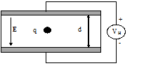 Figure 18.3: Part 9
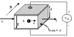 Figure 18.4: Example